


Optimize PCB Design for Maximum RF Performance Using a Board Footprint Simulation
When interfacing a coaxial connector with a PCB, transitioning between two transmission line types can hinder RF performance if not handled properly. Having the proper geometry on the PCB when moving from a coaxial to PCB line, such as microstrip or stripline, is critical. The PCB footprint for the coaxial connector must be optimized to ensure peak RF performance.
Optimizing Connector Footprint with CST and HFSS
Addressing the challenges of interfacing coaxial connectors with PCB layouts requires careful attention to PCB Footprint and stack-up considerations. With this scrutiny, a board footprint simulation can be used to maximize RF performance.
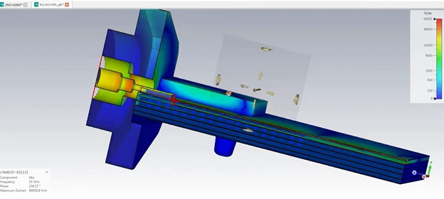
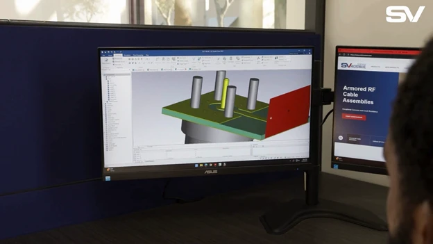
Optimizing the connector footprint with simulation tools is a key part of the process. SV uses simulation tools such as CST and HFSS to understand how best to optimize.
Solving PCB footprint challenges begins with understanding that every PCB stack and RF connector interacts differently. To address this, we conduct multiple iterations to tune each feature and achieve peak performance.
We want our connectors to work as best as possible for you, so we’re happy to assist early in the design phase, before simple design mistakes can lead to expensive board re-spins.
How to Optimize Connector Footprints On Your Own
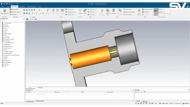
We also offer fully encrypted 3D models that can be employed directly into CST and HFSS if you prefer to handle the footprint design yourself. These CST and HFSS model footprints obscure the proprietary internal design of our parts while still giving full electrical performance within your simulation environment.
If you will be handling the footprint design and optimization yourself, following internal PCB footprint design guidelines, maintaining awareness of PCB footprint standards, and referencing a PCB footprint checklist are all crucial. These can support proper footprint development and reduce the risk of performance issues.
Interested In Board Footprint Support?
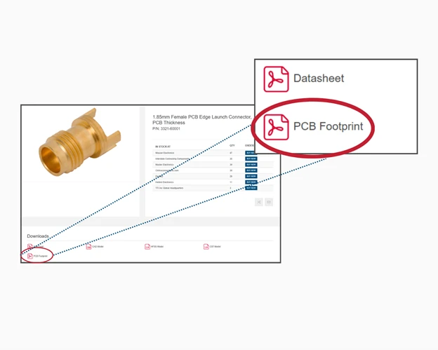
If you’d like a custom PCB footprint, we offer a request form. This form can be found in the downloads section of any PCB connector, as shown above.
Watch our video today for more information.
recent releases
Optimize PCB Design for Maximum RF Performance Using a Board Footprint Simulation
When interfacing a coaxial connector with a PCB, transitioning between two transmission line types can hinder RF performance if not handled properly. Having the proper geometry on the PCB when moving from a coaxial to PCB line, such as microstrip or stripline, is critical. The PCB footprint for the coaxial connector must be optimized to ensure peak RF performance.
Optimizing Connector Footprint with CST and HFSS
Addressing the challenges of interfacing coaxial connectors with PCB layouts requires careful attention to PCB Footprint and stack-up considerations. With this scrutiny, a board footprint simulation can be used to maximize RF performance.
Optimizing the connector footprint with simulation tools is a key part of the process. SV uses simulation tools such as CST and HFSS to understand how best to optimize.
Solving PCB footprint challenges begins with understanding that every PCB stack and RF connector interacts differently. To address this, we conduct multiple iterations to tune each feature and achieve peak performance.
We want our connectors to work as best as possible for you, so we’re happy to assist early in the design phase, before simple design mistakes can lead to expensive board re-spins.
How to Optimize Connector Footprints On Your Own
We also offer fully encrypted 3D models that can be employed directly into CST and HFSS if you prefer to handle the footprint design yourself. These CST and HFSS model footprints obscure the proprietary internal design of our parts while still giving full electrical performance within your simulation environment.
If you will be handling the footprint design and optimization yourself, following internal PCB footprint design guidelines, maintaining awareness of PCB footprint standards, and referencing a PCB footprint checklist are all crucial. These can support proper footprint development and reduce the risk of performance issues.
Interested In Board Footprint Support?
If you’d like a custom PCB footprint, we offer a request form. This form can be found in the downloads section of any PCB connector, as shown above.
Watch our video today for more information.